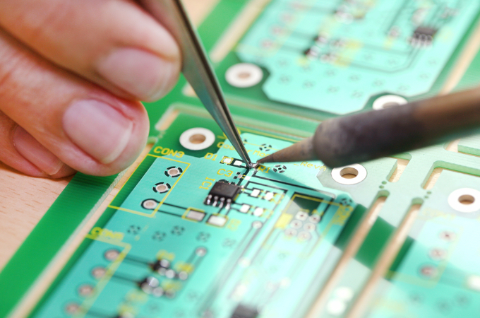
Although you have been able to print drawing patterns and conductor paths from PCB layout that has been completed in the design, does not mean the PCB Assembly process has been completely. Because basically, you’ve made it just a PCB layout printed on paper, not to the copper layer of the actual PCB. Therefore, the image and path pattern of the conductor of the printed PCB layout must be moved to the PCB copper layer in its original form.
There are several methods that can be used to transform the image pattern and conductor path from the PCB layout printing to the original PCB. Or you can use a PCB Assembly Services to do it.
The methods are as follows:
- Move the image pattern and the path of the conductor from the PCB layout with the chemical technique.
In the process of making PCB with the chemical technique used Positive chemicals 20 to coat the surface of copper PCB. Positive chemicals 20 can be obtained from electronics stores or at chemicals stores. Using Positive chemicals 20 allows you to create small, thin and tightly sized PCB layouts to each other.
- Moving the pattern of drawing and conductor path from PCB layout with screen printing technique.
One of the reasons why you should choose this screen printing technique is by using screen printing technique you can reduce the cost of making PCB when PCB sheet used is very much. Because, with only one process of transferring the image pattern from paper to sekrin, you can print the pattern of conductor path directly on top of PCB sheet repeatedly. However, in the process of making PCBs by using screen printing techniques, the thing to note is the ink material or the printed paint must be waterproof. Because if the material is not waterproof print when the process of dissolution with Ferri Chlorite (FeCl4) PCB conductor path will come dissolved. Therefore the type of ink or paint used should be made of oil or other chemicals that will not dissolve in water
- Move the drawing pattern and the path of the conductor from the PCB layout with the PCB transfer paper. Besides using chemical techniques and screen printing techniques, you can also use other media to move the PCB layout image pattern, by using PCB transfer paper. Compared with chemical techniques and screen printing techniques this way can be said much more easily, cheap and practical so suitable for students and students who have a limited cost. PCB transfer papers can be purchased at stores that sell electronics components.
The form of PCB transfer paper is the same as the paper in general which is plain white and unlined. However, the difference between plain paper and PCB transfer paper is on the paper-forming material. PCB transfer papers are specially designed to be able to move the PCB series path pattern from the toner (the ink powder commonly used in laser printers or copiers) to the PCB copper layer.